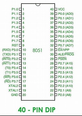
A 40 pin Dual Inline Package 8051 microcontroller is used (DIP). These 40 pins are used for a variety of tasks, including read, write, I/O operations, interrupts, and more. Eight pins on each of the four I/O ports of the 8051 may be set up as inputs or outputs depending on the logic state of the pins. Thus, I/O ports are the only use of 32 of these 40 pins. The remaining pins are reserved for the following: VCC, GND, XTAL1, XTAL2, RST, ALE, EA', and PSEN'.
Pin diagram of 8051 microprocessor is as given below:
Description of Pins:
Port 1: Pin 1 to Pin 8
Port 1's designated pins 1 through 8 are used for basic I/O activities. Depending on the logic control, they can be set up as input or output pins; for example, if logic zero () is applied to the I/O port, the pin will function as an output pin, and if logic one (), the pin would function as an input pin. These pins are also known as P1.0 to P1.7, where P1 denotes a pin in port 1 and the number after the period denotes the pin number, with 0 denoting the first pin of the port. P1.0 denotes the first pin of port 1, P1.1 the second pin, and so on. These pins may move in both directions.
Pin 9 (RST) –
Reset pin. It is an active-high, input pin. Therefore, if the RST pin is high for a minimum of 2 machine cycles, the microcontroller will reset i.e., it will close and terminate all activities. It is often referred as “power-on-reset” pin because it is used to reset the microcontroller to its initial values when power is on (high).
Pin 10 to Pin 17 (Port 3) –
The port 3 pins, commonly known as P3.0 to P3.7, are located from pin 10 to pin 17. These pins can be used as general input or output pins and are comparable to port 1. These pins may move in both directions.
These pins also serve the following extra purposes:
Port3: -P3.0 (RXD):
10th pin is RXD (serial data receive pin) which is for serial input. Through this input signal microcontroller receives data for serial communication.
Port3:P3.1 (TXD):
11th pin is TXD (serial data transmit pin) which is serial output pin. Through this output signal microcontroller transmits data for serial communication.
Port3:P3.2 and P3.3 (INT0′, INT1′):
12th and 13th pins are for External Hardware Interrupt 0 and Interrupt 1 respectively. When this interrupt is activated(i.e. when it is low), 8051 gets interrupted in whatever it is doing and jumps to the vector value of the interrupt (0003H for INT0 and 0013H for INT1) and starts performing Interrupt Service Routine (ISR) from that vector location.
Port3: P3.4 and P3.5 (T0 and T1):
14th and 15th pin are for Timer 0 and Timer 1 external input. They can be connected with 16-bit timer/counter.
Port3:P3.6 (WR’):
16th pin is for external memory write i.e. writing data to the external memory.
Port3:P3.7 (RD’):
17th pin is for external memory read i.e. reading data from external memory.
Pin 18 and Pin 19 (XTAL2 And XTAL1) –
These pins are connected to an external oscillator which is generally a quartz crystal oscillator. They are used to provide an external clock frequency of 4MHz to 30MHz.
Pin 20 (GND) –
This pin is connected to the ground. It has to be provided with 0V power supply. Hence it is connected to the negative terminal of the power supply.
Pin 21 to Pin 28 (Port 2) –
Pin 21 to pin 28 are port 2 pins also referred to as P2.0 to P2.7. When additional external memory is interfaced with the 8051 microcontroller, pins of port 2 act as higher-order address bytes. These pins are bidirectional.
Pin 29 (PSEN) –
PSEN stands for Program Store Enable. It is output, active-low pin. This is used to read external memory.
Pin 30 (ALE/ PROG) –
Address Latch Enable is referred to as ALE. It is an active-high input pin. In situations where there are many memory chips being utilized, this pin is used to differentiate between them. Additionally, it is employed to demultiplex the port 0's multiplexed address and data signals.
This pin serves as the program pulse input during EPROM programming, also known as flash programming (PROG).
Pin 31 (EA/ VPP) –
External Access is short for input. It is employed to turn on and off external memory interface. Since the 8051 has on-chip ROM to store programs, EA is coupled to Vcc. The EA pin is linked to the GND for other members of the 8031 and 8032 families that lack an on-chip ROM.
Pin 32 to Pin 39 (Port 0): –
Port 0 pins, often known as P0.0 to P0.7, are pins 32 to 39. They are pins with bidirectional input and output. There are no internal pull-ups there. Pull-up registers are therefore employed as external pull-ups. Because the 8051 multiplexes address and data through port 0 to conserve pins, port 0 is also known as AD0-AD7.
Pin 40 (VCC) –
This pin provides power supply voltage of (+5v) to the circuit.


